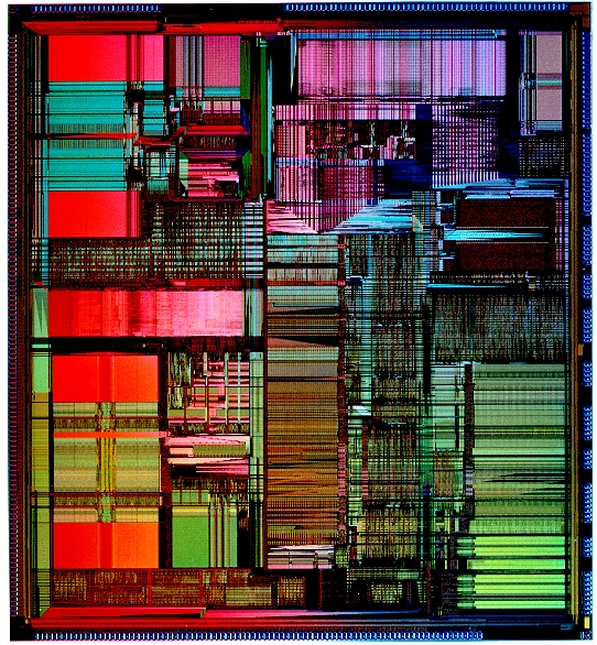
One of the biggest shortcomings of silicon is that it can only be made so thin because its material properties are fundamentally limited to three dimensions [3D]. For this reason, two-dimensional [2D] semiconductors—so thin as to have almost no height—have become an object of interest to scientists, engineers and microelectronics manufacturers.
Thinner chip components would provide greater control and precision over the flow of electricity in a device, while lowering the amount of energy required to power it. A 2D semiconductor would also contribute to keeping the surface area of a chip to a minimum, lying in a thin film atop a supporting silicon device.
But until recently, attempts to create such a material have been unsuccessful.
Now, researchers at the University of Pennsylvania School of Engineering and Applied Science have grown a high-performing 2D semiconductor to a full-size, industrial-scale wafer. In addition, the semiconductor material, indium selenide (InSe), can be deposited at temperatures low enough to integrate with a silicon chip.
“For the purposes of an advanced computing technology, the chemical structure of 2D InSe needs to be exactly 50:50 between the two elements. The resulting material needs a uniform chemical structure over a large area to work,” says Song.
The team achieved this groundbreaking purity using a growth technique called “vertical metal-organic chemical vapor deposition” (MOCVD). Previous research had attempted to introduce the indium and selenium in equal quantities and at the same time. Song demonstrated, however, that this method was the source of undesirable chemical structures in the material, producing molecules with varying ratios of each element. MOCVD, by contrast, works by sending the indium in a continuous stream while introducing the selenium in pulses.


